Got a feeling this could be a bit of an epic adventure .... it's showing signs already ...
Technos 2 pcb board set and looks similar to Double Dragon which I've fixed a few of. Maybe that'll come in handy, maybe not.
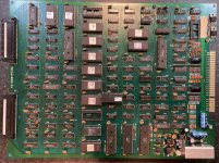
Not a game I've ever owned or played before but seems to have plenty of admirers out there so looking forward to getting it running... Here's the top pcb ...

First up a little clean and it scrubbed up nicely, no obvious signs of damage or previous repairs .... and I was quite hopeful of a working game ... but alas it booted to absolutely nothing ... black screen, no sound, nothing ... no sync on the monitor ... ok well might not be that bad, maybe just missing it's sync and sure enough no sync signal on the Jamma edge pin P ...
At this point I wasn't hopeful of schematics and thought I may have to use double dragon schematics to help here as it probably uses some similar circuitry. But there are schematics out there (Solar Warrior) which is some good news!
Straight forward catch here to begin ...
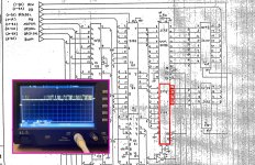
The CSYNC signal is generated by an XOR gate within IC60 (LS86) on the bottom PCB. HSYNC and VSYNC are fed into pins 1 and 2, with the combined CSYNC signal output on pin 3.
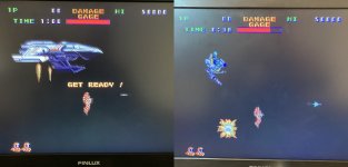
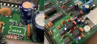
Both input signals were present and correct (15.6kHz & 57 Hz) but there was no output on pin 3. A quick piggyback got me a picture on screen so I replaced the LS86 which restored CSYNC to the Jamma edge connector ... hooray ... unfortunately though now all I get is garbage on the screen ... boo

OK clearly game code not running ... so firstly I need to check the Program ROMs ...and then CPU activity. And I quickly found a couple of things which got my hopes up again for a quick fix ... While checking the program roms I noticed one ROM (one of the sub cpu prog roms) looked to have a bent leg in the socket ... which was confirmed when removed.

ROM verified fine and went back in the socket (leg straightened) ... The other program ROMs also verified good so was hopeful of improvement, but this made zero difference and I'm still getting the same garbage on screen...
Next I go looking at the CPU's ... this board has three of them and all three are socketed ... there are 2x 6809E and 1x 6089 ... but I want to know for sure which one does what, so a bit of research later and now I know it has a main cpu - IC89 (6809E) a sub cpu - IC30 (6809E) and a sound cpu - IC62 (6809) ... except ... someone must've been swapping these around on this board at some point because the 6809 is in the main cpu socket !! and a 6809E is in the sound cpu socket !! This is not correct because these are not pin compatible despite being very closely related. Soooo I think ok ... this is the problem, and I swap the cpu's back around making sure the correct one is in the correct socket ... and boot up .... nah still the same garbage on screen. Hmmmm maybe one or more of these cpu's are toast if someone's been playing around with them. So I replace all 3 cpu's with some of my own CPU's and again it makes no difference. So hopes of the quick fix diminish and now I've got some nagging worries that if someone has been swapping cpu's about what else have they been up to ??!!
Anyway start scoping the main CPU pins and all looks ok ... no issues with reset or halt, clocks are all present and correct ... Address and Data lines toggling away ... then moved to the nearby LS245 (IC88) buffering its data, and all the signals between it and the CPU look fine but one signal on the other side of the buffer (D3 on the databus) looks really iffy - mostly noisy low with a few thin spikes up to about 2v max here and there ... ok what's going on here ... looked like it was being pulled low and yeah got the multimeter out and found a 23 ohm short between that pin and ground. My heart sank a little bit at this point because I realised that this signal was going to pop up on a number of IC's it being on the data bus

At least 7 pages of the schematics (as you can see above) where the Data Bus appears ... so loads of buffers and latches no doubt ... first thing i did was disconnect the bottom pcb which confirmed the short on the top pcb ... then I checked every page of the top pcb schematics and found 16 IC's connected to D3 stuck a piece of yellow tape on each one ... I've made them stand out more on the pic below ... Every one of them had the partial short to ground on the pin carrying the D3 signal. But which one was the bad one with the internal short? Or was there a small bridge somewhere on a trace? I checked all the traces I could see and didn't see any issues with a bridge, so unless it was a trace bridge under a chip, it was a chip itself shorted ...
So my approach here was to make small strategic cuts in the traces to split the marked IC's up into groups and narrow down the short to certain areas and IC's ... I've also marked below the general route of the traces (in blue) connecting this signal on these IC's .... and the first cut (marked with the red X) was to isolate the five IC's on the left hand side of the board ...

I wanted to do this using the smallest unnoticeable cuts as possible and ones that could be easily reinstated and not look obvious, so looked for vias on the solder side where I could cut the trace right next to the via and then repair later by just popping a bit of solder in the via with a drip out over the side to rejoin to the track ... that was the idea anyway !
In the end I reinforced the rejoin with a tiny bit of wire just to make sure .. looked reasonably subtle in the end, looking from a normal distance, when touched up with a little bit of solder mask ...

So that first cut removed all 23 ohm shorts on the IC's on the left hand side of the board, ruling them out as the culprit and moving attention to the eleven IC's on the right hand side ... The next cut was made just below the LS244 above the dipswitches, splitting the 11 IC's into a group of 5 below and 6 above the cut ... did this one right at the bottom of the IC leg between it and the trace, again easy enough to fill that tiny break with solder and it not look obviously messy ...

This removed the short on the six IC's above that cut and narrowed the culprit down to one of the five IC's below that cut...
Cut 3 isolated the 2x LS245's lowest down (on the next pic) and they lost the short, which left the 2x LS244's and 1x LS174 as the three remaining suspects ...
Cut 4 isolated the 174 from the 244's and it kept the short while the LS244's lost it ... gotcha

So 4 tiny trace cuts found the murderer !! IC79 (LS174) and I confirmed it with a snip of its offending D3 signal carrying leg, and proved the short was 100% on the chip itself ...
Replaced the chip, and fixed all the tiny trace breaks I'd made ... so with all connections re-made and no more partial shorts I fired it up feeling quite happy with myself ...

And now all I'm getting is a solid blue (sometimes purple) screen
Had a quick look to make sure that D3 signal is now normal looking and it is, and double checked all my traces, which are good ...
Ended the first session on this board here, with the feeling this one could have quite a number of issues ...... we'll see ...
Technos 2 pcb board set and looks similar to Double Dragon which I've fixed a few of. Maybe that'll come in handy, maybe not.
Not a game I've ever owned or played before but seems to have plenty of admirers out there so looking forward to getting it running... Here's the top pcb ...
First up a little clean and it scrubbed up nicely, no obvious signs of damage or previous repairs .... and I was quite hopeful of a working game ... but alas it booted to absolutely nothing ... black screen, no sound, nothing ... no sync on the monitor ... ok well might not be that bad, maybe just missing it's sync and sure enough no sync signal on the Jamma edge pin P ...
At this point I wasn't hopeful of schematics and thought I may have to use double dragon schematics to help here as it probably uses some similar circuitry. But there are schematics out there (Solar Warrior) which is some good news!
Straight forward catch here to begin ...
The CSYNC signal is generated by an XOR gate within IC60 (LS86) on the bottom PCB. HSYNC and VSYNC are fed into pins 1 and 2, with the combined CSYNC signal output on pin 3.
Both input signals were present and correct (15.6kHz & 57 Hz) but there was no output on pin 3. A quick piggyback got me a picture on screen so I replaced the LS86 which restored CSYNC to the Jamma edge connector ... hooray ... unfortunately though now all I get is garbage on the screen ... boo
OK clearly game code not running ... so firstly I need to check the Program ROMs ...and then CPU activity. And I quickly found a couple of things which got my hopes up again for a quick fix ... While checking the program roms I noticed one ROM (one of the sub cpu prog roms) looked to have a bent leg in the socket ... which was confirmed when removed.
ROM verified fine and went back in the socket (leg straightened) ... The other program ROMs also verified good so was hopeful of improvement, but this made zero difference and I'm still getting the same garbage on screen...
Next I go looking at the CPU's ... this board has three of them and all three are socketed ... there are 2x 6809E and 1x 6089 ... but I want to know for sure which one does what, so a bit of research later and now I know it has a main cpu - IC89 (6809E) a sub cpu - IC30 (6809E) and a sound cpu - IC62 (6809) ... except ... someone must've been swapping these around on this board at some point because the 6809 is in the main cpu socket !! and a 6809E is in the sound cpu socket !! This is not correct because these are not pin compatible despite being very closely related. Soooo I think ok ... this is the problem, and I swap the cpu's back around making sure the correct one is in the correct socket ... and boot up .... nah still the same garbage on screen. Hmmmm maybe one or more of these cpu's are toast if someone's been playing around with them. So I replace all 3 cpu's with some of my own CPU's and again it makes no difference. So hopes of the quick fix diminish and now I've got some nagging worries that if someone has been swapping cpu's about what else have they been up to ??!!
Anyway start scoping the main CPU pins and all looks ok ... no issues with reset or halt, clocks are all present and correct ... Address and Data lines toggling away ... then moved to the nearby LS245 (IC88) buffering its data, and all the signals between it and the CPU look fine but one signal on the other side of the buffer (D3 on the databus) looks really iffy - mostly noisy low with a few thin spikes up to about 2v max here and there ... ok what's going on here ... looked like it was being pulled low and yeah got the multimeter out and found a 23 ohm short between that pin and ground. My heart sank a little bit at this point because I realised that this signal was going to pop up on a number of IC's it being on the data bus
At least 7 pages of the schematics (as you can see above) where the Data Bus appears ... so loads of buffers and latches no doubt ... first thing i did was disconnect the bottom pcb which confirmed the short on the top pcb ... then I checked every page of the top pcb schematics and found 16 IC's connected to D3
stuck a piece of yellow tape on each one ... I've made them stand out more on the pic below ... Every one of them had the partial short to ground on the pin carrying the D3 signal. But which one was the bad one with the internal short? Or was there a small bridge somewhere on a trace? I checked all the traces I could see and didn't see any issues with a bridge, so unless it was a trace bridge under a chip, it was a chip itself shorted ... So my approach here was to make small strategic cuts in the traces to split the marked IC's up into groups and narrow down the short to certain areas and IC's ... I've also marked below the general route of the traces (in blue) connecting this signal on these IC's .... and the first cut (marked with the red X) was to isolate the five IC's on the left hand side of the board ...
I wanted to do this using the smallest unnoticeable cuts as possible and ones that could be easily reinstated and not look obvious, so looked for vias on the solder side where I could cut the trace right next to the via and then repair later by just popping a bit of solder in the via with a drip out over the side to rejoin to the track ... that was the idea anyway !
In the end I reinforced the rejoin with a tiny bit of wire just to make sure .. looked reasonably subtle in the end, looking from a normal distance, when touched up with a little bit of solder mask ...
So that first cut removed all 23 ohm shorts on the IC's on the left hand side of the board, ruling them out as the culprit and moving attention to the eleven IC's on the right hand side ... The next cut was made just below the LS244 above the dipswitches, splitting the 11 IC's into a group of 5 below and 6 above the cut ... did this one right at the bottom of the IC leg between it and the trace, again easy enough to fill that tiny break with solder and it not look obviously messy ...
This removed the short on the six IC's above that cut and narrowed the culprit down to one of the five IC's below that cut...
Cut 3 isolated the 2x LS245's lowest down (on the next pic) and they lost the short, which left the 2x LS244's and 1x LS174 as the three remaining suspects ...
Cut 4 isolated the 174 from the 244's and it kept the short while the LS244's lost it ... gotcha
So 4 tiny trace cuts found the murderer !! IC79 (LS174) and I confirmed it with a snip of its offending D3 signal carrying leg, and proved the short was 100% on the chip itself ...
Replaced the chip, and fixed all the tiny trace breaks I'd made ... so with all connections re-made and no more partial shorts I fired it up feeling quite happy with myself ...
And now all I'm getting is a solid blue (sometimes purple) screen
Had a quick look to make sure that D3 signal is now normal looking and it is, and double checked all my traces, which are good ...
Ended the first session on this board here, with the feeling this one could have quite a number of issues ...... we'll see ...