Fixing an Alcon/Slap Fight PCB

myPinballs

Active member
Feedback
16 (100%)
Credits
693CR
Starting my next board repair. This time a slap fight/alcon board. Bought in a pile of unseen unknown random stuff. Not working

Replaced ribbon cables and roms and got to this so far. Think i can make out a 'RAM Test ok message' but the screen image is blurred and not synced great. Better than a blank screen which is what started with though.

IMG_9699.JPG
 

myPinballs

Active member
Feedback
16 (100%)
Credits
693CR
Not having a great time with this one currently. Lost the ram check message and now stuck on the all zeros page.

I did find some bodge repair attempt around the clock gen section, so replacing all this. Pic below is after i removed the 74S04 ic and started to remove the old parts.

IMG_9707.jpg


And I found out the crystal installed was the wrong value 32mhz instead of a 36mhz. Also want to check the resistor and cap values of the clock generation in case these are wrong also. Currently I have 1.2k and 15pF.

Could anyone with a working board check this for me?
 

myPinballs

Active member
Feedback
16 (100%)
Credits
693CR
Small update. I changed the clock circuit parts using the values i had installed before 1.2K , 15pf and using a 36Mhz crystal.

IMG_9712.jpg


After doing this i was able to sometimes get a stable picture, but not always. I'm thinking this is kind of progress, but i'm a bit stuck now as to how to work out what's causing the loss of picture and also what's would stop the board from starting the ram test.

If anyone knows what needs to be working chip wise for the ram test to start i'd love to know. I'm assuming the main cpu section, i.e Z80 8Q, 2 roms 8N, 8P and the ram 8M. Think i'm going to socket 8M next and change to see if any difference. I should say i can't find any signal line issues with address or data lines in this area.

I'm wondering if the picture i sometimes get could help identify where the issue lies but not sure

This is what is shown

IMG_9719.jpg


myPinballs2017-08-31 19:26:24
 

Judder

Active member
Feedback
2 (100%)
Credits
992CR
How you getting on?

I'm chasing a similar set of problems with my Slap Fighter set so thought it might be more helpful to join your thread and try and debug these boards - here's where I am up to

Standard boot = blank green screen (the screen indicates some sort of activity)

If I disconnect the board connector lead from the CPU board (assumed to be the one connected to the Jamma connector) to the Video board (assumed to be the secondary board) as per the Red arrow below I get a memory failure which makes sense as there is now no memory connected

The fact the error specifically talks about the range of the RAM error implies to me that the Z80 CPU on the CPU board (Green arrow) is working *but that might be a false assumption

SlapFightErrorSmall.jpg


SlapFightBoardsLow.jpg


So far I have found this fix log from JammArcade

http://www.jammarcade.net/slap-fight-bootleg-repair-log/

but none of those seem to obviously apply as I appear to have the 36Mhz crystal and there is activity there

Thoughts from anyone as to next steps very welcome!

Judder2018-01-14 16:51:31
 

myPinballs

Active member
Feedback
16 (100%)
Credits
693CR
Hi,

Thanks for the message and yes it would be great to get both our board faults solved. Its not a bad time for me to look at mine again actually as i just finished (before christmas) my mk2 cpu and sound board repairs. I parked the slap fight boards and went back to the mk2 sound board to finish that off. Thats now completed and 100% working so i could look at my slap fight boards again.

I was iirc a bit stuck, as i wasn't able to get very far in the boot process. The board came up with what looked like the start of a ram test, so i think i was about to change some rams ics to see what happened. Need to refresh my memory on the quality of the schematics. Can't remember if they were complete or not. I know they were redrawn by someone i think.
 

Mitchell Gant

Active member
vacBacker
Feedback
2 (100%)
Credits
884CR
myPinballs said:
Hi,
Need to refresh my memory on the quality of the schematics. Can't remember if they were complete or not. I know they were redrawn by someone i think.

I traced out most of a Tiger Heli and then a Slap Fight PCB with a multimeter and some patience:

http://www.ukvac.com/forum/tiger-heli-schematics-pdfclear-but-may-be-wrong_topic340113.html

They're the same apart from the wait state logic, and on some PCBs I've seen 'LS194 shift registers instead of 'LS299s for the graphics pixel shifters.

Hope that helps you.
 

Judder

Active member
Feedback
2 (100%)
Credits
992CR
Excellent - and thanks Mitchell Gant for the schematics +1

Well I spent a little bit more time on my set last night and here's where I got to

1. Connecting up a logic probe

Quick note for my future self, but you can use the big capacitors at the edge of the Video board to provide a good +5V and GND for the logic probe to use

2. Test Z80 Reset signal

So I logic probed pin 26 on the two Z80s (one on each board) and when turning the power supply on checked that they went through their correct power on process which is:

- Initial Low to reset chip (it's active low)

- Then High to let chip run

- Stay High

Both chips went through these processes correctly so that was a good start

3. Test Address and Data signals on EPROM groups

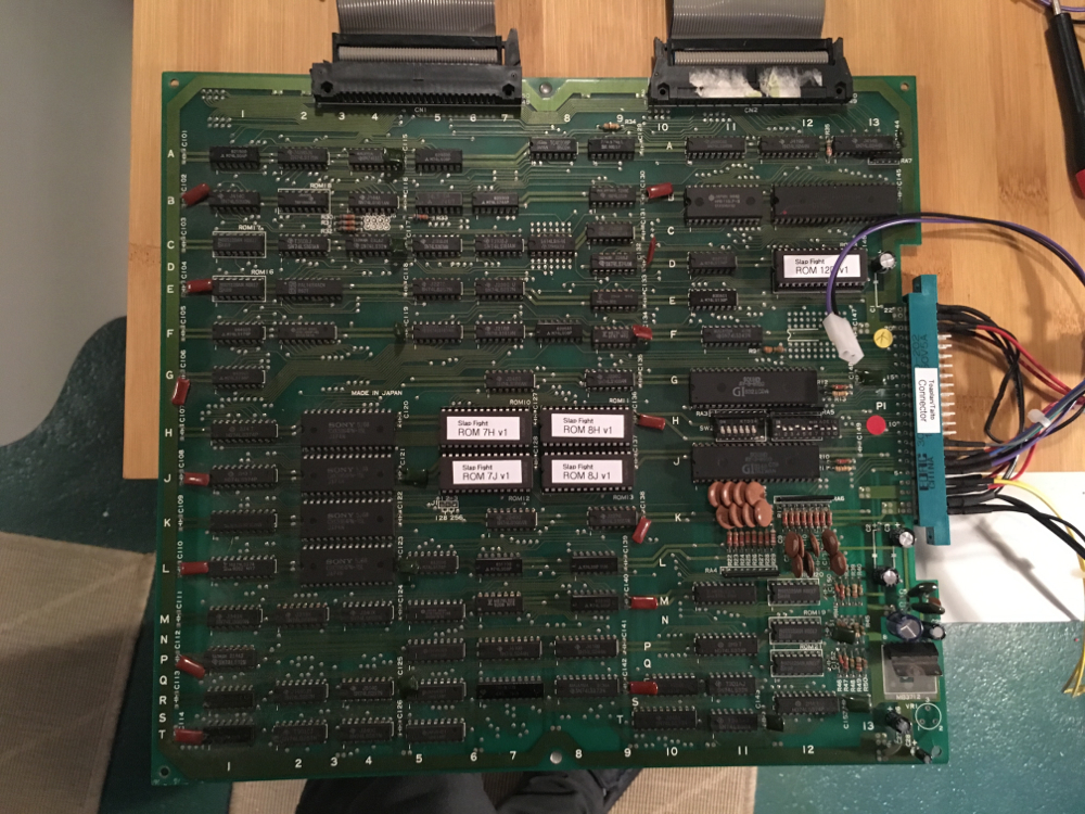
The EPROMs on the boards are grouped together based on their functions and cross referencing the Slap Fight driver in Mame here I worked out that the groupings are as follows:

CPU Board

A77_02 = Sound

A77_09, A77_10, A77_11, A77_12 = Sprites (confirmed in repair log referenced above)

Video Board

A77_00, A77_01 = Main CPU

A77_05, A77_06, A77_07, A77_08 = Tiles (from Mame driver)

A77_03, A77_04 = Chars (from Mame driver

So next step was to test the address and data lines on each 'group' of EPROMs and see if they are getting data as expected (pulsing High / Low signals)

4. Sprites (A9, A10, A11, A12)

From a video I had seen online about another Slap Fight repair, in their case the 74LS32 chips on the CPU board up by position 11 had blown the 4 x 74LS166AP parallel load, serial out 8bit shift registers which power the sprite ROM causing the clock signal shorted high (74LS166AP)

So I ran the probe across these 27128 chips and found that a number of the address registers where showing no state (neither High or Low)

[font="Courier New, Courier, mono"]27128[/font]

[font="Courier New, Courier, mono"]
[/font]

[font="Courier New, Courier, mono"]H Vpp Vcc H[/font]

[font="Courier New, Courier, mono"]H A12 /PGM H[/font]

[font="Courier New, Courier, mono"]H A7 A13 H[/font]

[font="Courier New, Courier, mono"]H A6 A8 L[/font]

[font="Courier New, Courier, mono"]H A5 A9 L[/font]

[font="Courier New, Courier, mono"]X A4 A11 H[/font]

[font="Courier New, Courier, mono"]X A3 /OE L[/font]

[font="Courier New, Courier, mono"]X A2 A10 H[/font]

[font="Courier New, Courier, mono"]X A1 /CE L[/font]

[font="Courier New, Courier, mono"]HL A0 D7 HL[/font]

[font="Courier New, Courier, mono"]HL D0 D6 HL[/font]

[font="Courier New, Courier, mono"]HL D1 D5 HL[/font]

[font="Courier New, Courier, mono"]HL D2 D4 HL[/font]

[font="Courier New, Courier, mono"]L GND D3 HL[/font]

I piggy backed some 74LS32 chips on top of the two 74LS32 chips at position 11 on the CPU board, but no luck so I'm going to order some 74LS166 chips and try piggy backing those. In the mean time I can start probe testing them too to see if they are sending out signals correctly

5. Audio (A2)

The 2nd part of the board self test is the AUDIO test, and as we can see that the self test is running by pulling out the board interconnectors I wondered if this may also be a problem

[font="Courier New, Courier, mono"]2764[/font]

[font="Courier New, Courier, mono"]
[/font]

[font="Courier New, Courier, mono"]H Vpp Vcc H[/font]

[font="Courier New, Courier, mono"]X A12 /PGM H[/font]

[font="Courier New, Courier, mono"]XD A7 N/C H[/font]

[font="Courier New, Courier, mono"]HL A6 A8 HL[/font]

[font="Courier New, Courier, mono"]HL A5 A9 X[/font]

[font="Courier New, Courier, mono"]HL A4 A11 X[/font]

[font="Courier New, Courier, mono"]HL A3 /OE L[/font]

[font="Courier New, Courier, mono"]HL A2 A10 X[/font]

[font="Courier New, Courier, mono"]HL A1 /CE X[/font]

[font="Courier New, Courier, mono"]X A0 D7 HL[/font]

[font="Courier New, Courier, mono"]HL D0 D6 HL[/font]

[font="Courier New, Courier, mono"]HL D1 D5 HL[/font]

[font="Courier New, Courier, mono"]HL D2 D4 HL[/font]

[font="Courier New, Courier, mono"]L GND D3 HL[/font]

So here again we appear to have address problems (A0, A7, A9, A10, A11, A12) so I tested the connectivity of the EPROM pins to their corresponding solder on the bottom of the board, and they all appear fine

Chip Enable is also NOT Low here which means the chip isn't enabled so could be why the self test just freezes

6. Main CPU (A0, A1)

All fine - phew! At least something is OK

[font="Courier New, Courier, mono"]27128[/font]

[font="Courier New, Courier, mono"]
[/font]

[font="Courier New, Courier, mono"]Vpp Vcc[/font]

[font="Courier New, Courier, mono"]A12 /PGM[/font]

[font="Courier New, Courier, mono"]A7 A13[/font]

[font="Courier New, Courier, mono"]A6 A8[/font]

[font="Courier New, Courier, mono"]A5 A9[/font]

[font="Courier New, Courier, mono"]A4 A11[/font]

[font="Courier New, Courier, mono"]A3 /OE[/font]

[font="Courier New, Courier, mono"]A2 A10[/font]

[font="Courier New, Courier, mono"]A1 /CE[/font]

[font="Courier New, Courier, mono"]A0 D7[/font]

[font="Courier New, Courier, mono"]D0 D6[/font]

[font="Courier New, Courier, mono"]D1 D5[/font]

[font="Courier New, Courier, mono"]D2 D4[/font]

[font="Courier New, Courier, mono"]GND D3[/font]

7. Chars (A3, A4)

All fine

[font="Courier New, Courier, mono"]2764[/font]

[font="Courier New, Courier, mono"]
[/font]

[font="Courier New, Courier, mono"]H Vpp Vcc H[/font]

[font="Courier New, Courier, mono"]HL A12 /PGM H[/font]

[font="Courier New, Courier, mono"]HL A7 N/C L[/font]

[font="Courier New, Courier, mono"]HL A6 A8 HL[/font]

[font="Courier New, Courier, mono"]HL A5 A9 HL[/font]

[font="Courier New, Courier, mono"]HL A4 A11 HL[/font]

[font="Courier New, Courier, mono"]HL A3 /OE L[/font]

[font="Courier New, Courier, mono"]HL A2 A10 HL[/font]

[font="Courier New, Courier, mono"]HL A1 /CE L[/font]

[font="Courier New, Courier, mono"]HL A0 D7 HL[/font]

[font="Courier New, Courier, mono"]HL D0 D6 HL[/font]

[font="Courier New, Courier, mono"]HL D1 D5 HL[/font]

[font="Courier New, Courier, mono"]HL D2 D4 HL[/font]

[font="Courier New, Courier, mono"]L GND D3 HL[/font]

8. Tiles (A5, A6, A7, A8)

Again some problems here, but only aroudn the very high Address Registers (A11, A12, A13) so I'll try and trace back what is running those.

[font="Courier New, Courier, mono"]27128[/font]

[font="Courier New, Courier, mono"]
[/font]

[font="Courier New, Courier, mono"]L Vpp Vcc H[/font]

[font="Courier New, Courier, mono"]X A12 /PGM X[/font]

[font="Courier New, Courier, mono"]LH A7 A13 X[/font]

[font="Courier New, Courier, mono"]LH A6 A8 HL[/font]

[font="Courier New, Courier, mono"]LH A5 A9 HL[/font]

[font="Courier New, Courier, mono"]LH A4 A11 X[/font]

[font="Courier New, Courier, mono"]LH A3 /OE L[/font]

[font="Courier New, Courier, mono"]LH A2 A10 HL[/font]

[font="Courier New, Courier, mono"]LH A1 /CE L[/font]

[font="Courier New, Courier, mono"]LH A0 D7 HL[/font]

[font="Courier New, Courier, mono"]LH D0 D6 HL[/font]

[font="Courier New, Courier, mono"]LH D1 D5 HL[/font]

[font="Courier New, Courier, mono"]LH D2 D4 HL[/font]

[font="Courier New, Courier, mono"]L GND D3 HL[/font]

More updates as I get some time but hoping the the 74LS166 chips will help fix up the Sprite EPROM problems :)
 

myPinballs

Active member
Feedback
16 (100%)
Credits
693CR
My understanding is that the booting test is

1) RAM which should display all zeros on screen before a RAM ok message

2) ROM

3) Sound

So if the main cpu and its roms are functioning (clock,reset, address, data and other signal lines all test ok), then testing the rams would be the next logical step which should get you some sort of garbage on screen, or the all zeros screen. I would leave the sprite roms etc until you get passed the ram test.

Do you see any ram test when you power on?
 

Judder

Active member
Feedback
2 (100%)
Credits
992CR
myPinballs said:
My understanding is that the booting test is

1) RAM which should display all zeros on screen before a RAM ok message

2) ROM

3) Sound

So if the main cpu and its roms are functioning (clock,reset, address, data and other signal lines all test ok), then testing the rams would be the next logical step which should get you some sort of garbage on screen, or the all zeros screen. I would leave the sprite roms etc until you get passed the ram test.

Do you see any ram test when you power on?

Good call and yes your right about the RAM, ROM, SOUND test order (double checked on a video here)

Screen_Shot_2018-01-15_at_18.00.45.png


I get a failed RAM test when I disconnect the daughter board connector closest to the JAMMA connector, but that I figured was because the 2016 RAM on that board were now disconnected

SlapFightRAMCheckFail.jpg


With the board connected again I just get a flat screen, with occasionally a sprite or two bit randomly placed on it

Any thoughts how to test the memory on that board on which of the memory chips there are being tested (as I think off the top of my head it is soldered on)?

SlapFightBoardsRAM.jpg
 

Judder

Active member
Feedback
2 (100%)
Credits
992CR
myPinballs said:
What does the check ram error message actually say? I can't read it from your image.

RAM CHECK C800 ERROR

as far as I can tell but as above that's a forced error really as I have to disconnect the inter-board connector to get it to generate. Without it it's just a blank screen with the odd bit of sprite

BTW I have read and checked all of the EPROMs versus the Mame checksums and zip file so pretty sure they are all good (had to replace AA_02 as 3 legs snapped removing it!)

Just found this also which shows the correct boot sequence with the screen of 0s as you say, and then the three lines above

Judder2018-01-15 19:23:42
 

Mitchell Gant

Active member
vacBacker
Feedback
2 (100%)
Credits
884CR
Judder said:
myPinballs said:
What does the check ram error message actually say? I can't read it from your image.

RAM CHECK C800 ERROR

as far as I can tell but as above that's a forced error really as I have to disconnect the inter-board connector to get it to generate. Without it it's just a blank screen with the odd bit of sprite

C800 is the address of the sound CPU control port. If you say that you've disconnected the interboard connector that connects the main CPU to the Sound CPU, then I imagine you will always get that error with it disconnected!

The address lines on the tile graphics EPROMs will not necessarily be toggling, depending on what the game is doing at the time. I'd guess that game only accesses higher tile EPROM memory locations as it get further into the gameplay and newer backgrounds appear.

The main CPU has no way of accessing or testing the tile EPROMs, they're only selected from tile RAM output data and the graphic data goes directly to the pixel shift registers and then out to the monitor. You could remove all the tile and character EPROMs and the game would still pass self test. Though you would not be able to see anything on the monitor of course!
 

Mitchell Gant

Active member
vacBacker
Feedback
2 (100%)
Credits
884CR
Judder said:
The fact the error specifically talks about the range of the RAM error implies to me that the Z80 CPU on the CPU board (Green arrow) is working *but that might be a false assumption

That Z80 with the green arrow is the Sound CPU, NOT the main game CPU!
 

Judder

Active member
Feedback
2 (100%)
Credits
992CR
Mitchell Gant said:
That Z80 with the green arrow is the Sound CPU, NOT the main game CPU!

Great to know - as my first post said I was guessing which was which!

"If I disconnect the board connector lead from the CPU board (assumed to be the one connected to the Jamma connector) to the Video board (assumed to be the secondary board) as per the Red arrow below I get a memory failure which makes sense as there is now no memory connected"

So the board with the JAMMA connector is mainly the sound CPU (it obviously has the two AY sound chips on it)?

I had it as that was the Sound + main CPU and the other the video board, kind of like the three boards on Tron where you have CPU, Sound and Video, as it has most of the video EPROMs on there but guessing that was a wrong assumption
smiley9.gif


Going forwards any thoughts how to get past my current stop of the non-boot and where to focus?


Additional:


Reading the board schematics in the ROM section of the MAME driver versus the Machine Configuration sections I can see the CPUs match up as you say based on the speeds of the clock


1. Bottom Board

Z80B clock - 6.000MHz (36/6)

>>

/* basic machine hardware */

MCFG_CPU_ADD("maincpu",Z80, XTAL_36MHz/6) // 6MHz

2. PCB Layouts - Top Board

Z80A clock - 3.000MHz (36/12)

>>

MCFG_CPU_ADD("audiocpu", Z80, XTAL_36MHz/12) // 3MHz


Judder2018-01-16 00:02:27
 

myPinballs

Active member
Feedback
16 (100%)
Credits
693CR
My understanding of the 2 boards is

Bottom board (no edge connector) (CPU board)

CPU, Game Rom and Ram

Foreground Ram & Rom

Background Ram & Rom

Top Board (edge connector) (Sound Board)

Sound CPU, Sound Rom and Ram

Sprite Ram & Rom

What i'd like to know is how the ram test is displayed on screen. Are parts of the screen that show zeros related to individual rams being tested, as on other board sets the screen changes as each ram is loaded with test data.

Running in mame you just see a single full screen of zeros, no changing pattern. Does this mean only certain rams are checked?

I've also noted something different on my board in relation to the clock circuit in the redrawn schematics. My board seems to use 74LS194 ics in that area and doesn't match what is on page 3.

Also my board is not populated with the 68705 processor (6A) or chip 6B & 7A

myPinballs2018-01-16 10:14:55
 

Judder

Active member
Feedback
2 (100%)
Credits
992CR
Thanks for swapping that post above around - was just reading it starting to get all of us confused!

Is your board the 'alcon/slapfigh' board (with the Jamma pinout) or the 'slapfigha' board with the Tiger Heli type 22 pin out connector?

Here's a shot of the bottom of that board of the Tiger Heli style one which is quite a different layout from the Jamma one I have above

From the MAME driver

"This set comes from a different type of board with unique Taito ID code of "A76"
PCBs are labeled GX-006-A & GX-006-B It has a 22pin edge connector and closely
resembles the Tigher Heli PCB (shown above) with rom placement and components."


Screen_Shot_2018-01-15_at_18.02.37.png


John Bennett

Senior Member
vacBacker
Feedback
10 (100%)
Credits
5,003CR
If you've got sync problems, then is the horizontal/vertical count circuit working? I've hardly looked at many boards (and never a Slap Fight), but it seems normal (and logical) that the video circuit is the 'master' that drives the video hardware, including the sync signals and normally ~60Hz interrupts to the CPU. Dunno what happens in test modes etc if the interrupt stops or is jumping around (maybe it's not used - if so, ignore me). Might be worth checking these lower-rate clock signals anyway (they're derived from the main clock via counters and digital comparators), especially if the sync is going. John Bennett2018-01-16 12:18:45
 

Judder

Active member
Feedback
2 (100%)
Credits
992CR
Quick few more checks from me:

- Crystal = 36MHz checked with multimeter so that's all good [here's how to do it for reference]

- 74LS166 parallel -> serial loaders, pin 15 (shift load input) is high across all 4 chips so this according to the data sheet indicates that they are trying to run in serial input mode, where I'm pretty sure it should be low as per this repair log to enable the parallel input mode

I'll need to meter around to see what supplies that pin as the very good schematics from MG don't have that pin wired out yet - although the above log says it comes from a 74LS32

Addendum:

Decided that as there are so few Slap Fight / Alcon repair logs that searching for Tiger Heli fix logs might be a better idea

Success - found here another case of the 74LS166s playing up with a Tiger Heli but this time they've labelled the 74LS32 that relates to the problem - one to check tonight

Judder2018-01-17 10:25:15
 

myPinballs

Active member
Feedback
16 (100%)
Credits
693CR
Judder said:
Quick few more checks from me:

- Crystal = 36MHz checked with multimeter so that's all good [here's how to do it for reference]

- 74LS166 parallel -> serial loaders, pin 15 (shift load input) is high across all 4 chips so this according to the data sheet indicates that they are trying to run in serial input mode, where I'm pretty sure it should be low as per this repair log to enable the parallel input mode

I'll need to meter around to see what supplies that pin as the very good schematics from MG don't have that pin wired out yet - although the above log says it comes from a 74LS32

Addendum:

Decided that as there are so few Slap Fight / Alcon repair logs that searching for Tiger Heli fix logs might be a better idea

Success - found here another case of the 74LS166s playing up with a Tiger Heli but this time they've labelled the 74LS32 that relates to the problem - one to check tonight

0

From what you've mentioned before i'd suggest looking at the bottom board (edge connector) as something must mbe crashing your main cpu if you don't get any zero test screen when they are plugged in. As you get a ram error message with that ribbon disconnected that show that the main cpu is ok and possibly the sound cpu or something on the related address/databus is crashing the main one. Just my initial thoughts from the reported state of it.
 
Top