Juno first green lines

Lurch666

Active member
Feedback
21 (100%)
Credits
4,356CR
Thanks for the input dudes. This is now solved.

I couldn't find anywhere that could put bad data into DB6 without stopping the game from working.

@NivagSwerdna The game runs perfectly even with the green lines so I knew the CPU data was good.

So that left the output from pin 13 of the LS373 that only went to pin 20 of the custom 083 at E16 which I have already swapped out with a known good chip and the output pin 14 of the 4116 ram at D15.
So I snipped pin 14 and piggybacked a good 4116 onto D15 and the issue went away. Perfect graphics.
It looks like the ram test rom is missing something.
 
Last edited:

NivagSwerdna

Active member
Feedback
1 (100%)
Credits
794CR
Thanks for the input dudes. This is now solved.

I couldn't find anywhere that could put bad data into DB6 without stopping the game from working.

@NivagSwerdna The game runs perfectly even with the green lines so I knew the CPU data was good.

So that left the output from pin 13 of the LS373 that only went to pin 20 of the custom 083 at E16 which I have already swapped out with a known good chip and the output pin 14 of the 4116 ram at D15.
So I snipped pin 14 and piggybacked a good 4116 onto D15 and the issue went away. Perfect graphics.
It looks like the ram test rom is missing something.
Excellent
 

NivagSwerdna

Active member
Feedback
1 (100%)
Credits
794CR
Try and keep the 4116 and test it.

The read write for the RAM test is done at CPU speed whereas the screen rendering reads out the RAM out at the higher pixel clock rate. It would be interesting to see if it is being marginal
 

Retroman839

Senior Member
vacBacker
Feedback
13 (100%)
Credits
7,550CR
Custom konami cpu.
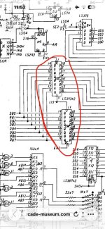
One of these 2 ls373’s
IMG_9493.jpeg
E15 ,E14 ?
I see DB6 goes to a couple of the 4116-2’s ?
C15 & D15…

I understand now the 4116’s are dual purpose very efficient !
through high speed
Timings . :)
Great fix man

Did you use ? Or is a schematic of this custom been drawn ? Was it required for this repair ?
 
Last edited:

NivagSwerdna

Active member
Feedback
1 (100%)
Credits
794CR
FWIW
The timings are a bit of a challenge here... the Konami 081 does the magic.
Essentially time is split into four sections, half for CPU and half for video and within those halves the time is split again since RAS/CAS muxes the addresses into the DRAM. The MXA/MXB signals from the Konami 081 are doing that part.
Because this all goes around fast enough the DRAM stays refreshed.
A byte encodes 2 pixels (nibble each) and the DRAM is in 16-bit wide arrangement so the Konami 083 loads two nibble pairs, i.e. 4 pixels (signal 119 from the Konami 081)
It's all a bit of a nightmare which is why I haven't gone back YET to the JF bootleg I was fixing!
No wonder there isn't much DRAM in Konami's of this era!
 
Last edited:

Retroman839

Senior Member
vacBacker
Feedback
13 (100%)
Credits
7,550CR
FWIW
The timings are a bit of a challenge here... the Konami 081 does the magic.
Essentially time is split into four sections, half for CPU and half for video and within those halves the time is split again since RAS/CAS muxes the addresses into the DRAM. The MXA/MXB signals from the Konami 081 are doing that part.
Because this all goes around fast enough the DRAM stays refreshed.
A byte encodes 2 pixels (nibble each) and the DRAM is in 16-bit wide arrangement so the Konami 083 loads two nibble pairs, i.e. 4 pixels (signal 119 from the Konami 081)
It's all a bit of a nightmare which is why I haven't gone back YET to the JF bootleg I was fixing!
No wonder there isn't much DRAM in Konami's of this era!

FWIW
The timings are a bit of a challenge here... the Konami 081 does the magic.
Essentially time is split into four sections, half for CPU and half for video and within those halves the time is split again since RAS/CAS muxes the addresses into the DRAM. The MXA/MXB signals from the Konami 081 are doing that part.
Because this all goes around fast enough the DRAM stays refreshed.
A byte encodes 2 pixels (nibble each) and the DRAM is in 16-bit wide arrangement so the Konami 083 loads two nibble pairs, i.e. 4 pixels (signal 119 from the Konami 081)
It's all a bit of a nightmare which is why I haven't gone back YET to the JF bootleg I was fixing!
No wonder there isn't much DRAM in Konami's of this era!
Also fascinating is
the usage of the timings of the monitor its self by the PCB’s video genaration .

So practical ..

Part of the game processing is
The timings occurring inside the monitors raster scanning

Fascinating that between cpu cycles those nano seconds the 4116’s are then processing video ..
and this sharing is controlled

Yeh I saw the mxA , MXB
First understanding all this is going on symiltainiously ( sorry no spell check on my phone !)

Yeh I soon realised thankfully that AI don’t know jack!

It said to rule Out 4116 being bad if game is running correctly ! 🤣

The duplicity is amazing..
and use of timings
 
Last edited:

NivagSwerdna

Active member
Feedback
1 (100%)
Credits
794CR
Under normal operation there is no low-impedance path from V_BB (-5V) or V_DD (+12V) to any of the digital output or input pads. Those two supplies terminate at transistor gates and the substrate/bulk region internally, while every pad's actual conducting path (source-to-drain) runs only between V_CC and V_SS. So electrically, -5V and +12V can influence how a pad switches (via gate drive or threshold bias) without ever being a destination the pad's current can flow to or from.

The only way that stops being true is if the chip itself has failed — die damage, latch-up, or a punched-through junction can create an unintended low-impedance path between rails that shouldn't normally be connected. But that's a fault condition, not a property of the intended design, and it's not something you'd rely on or expect to see on a healthy 4116.

So it depends... but I've done this many times with my logic analyser.

I would not recommending connecting pin 1 to pin 8... that's why i said "don't connect"
 

Retroman839

Senior Member
vacBacker
Feedback
13 (100%)
Credits
7,550CR
Under normal operation there is no low-impedance path from V_BB (-5V) or V_DD (+12V) to any of the digital output or input pads. Those two supplies terminate at transistor gates and the substrate/bulk region internally, while every pad's actual conducting path (source-to-drain) runs only between V_CC and V_SS. So electrically, -5V and +12V can influence how a pad switches (via gate drive or threshold bias) without ever being a destination the pad's current can flow to or from.

The only way that stops being true is if the chip itself has failed — die damage, latch-up, or a punched-through junction can create an unintended low-impedance path between rails that shouldn't normally be connected. But that's a fault condition, not a property of the intended design, and it's not something you'd rely on or expect to see on a healthy 4116.

So it depends... but I've done this many times with my logic analyser.

I would not recommending connecting pin 1 to pin 8... that's why i said "don't connect"

Where would you recommend connecting Gnd and +5 for this chip on this board ? 1&9 ?

I should mention I don’t have a Juno first .. Im hunting one

Nice to look at the schimatic and get an understanding of how it runs
Though.

Been thinking about the digital to analogue video recently because a board came up for sale with all green missing completly.

Which is why I took an interest in this particular repair and Glad I did because I now see and understand better the data bus lines, and this part of the pcb..
Also the diffrent timings .. going on.
High speed side of the video logic and the duplicity of the rams .
Basic io of multiplexers .. integral to this high speed shifting of bits that’s going on here ..

I feel like I’m seeing the matrix for the first time.

Like a giant car factory
 
Last edited:
Top