Yet another SubElectro MC type Fantazia/Pisces ???

cliff_poole

Active member
vacBacker
Feedback
6 (100%)
Credits
1,069CR
If the NVRAM on the philmurr daughterboard is still good, I'd probably find a high score save ROM set and stick with that, no need to use up 2114's then. Its great to have a high score goal to work towards on Galaxian type games, gives them an extra dimension.
 

NivagSwerdna

Active member
Feedback
1 (100%)
Credits
840CR
cliff_poole said:
If the NVRAM on the philmurr daughterboard is still good, I'd probably find a high score save ROM set and stick with that, no need to use up 2114's then. Its great to have a high score goal to work towards on Galaxian type games, gives them an extra dimension.
I'm aiming at Fantasia but I will keep the philmur save gadget for possible employment in a Galaxian. I haven't actually managed to find much time to actually play many games, too busy trying to fix them!

My original goal was to fix up my cocktail to have RocnRope... That project is now about 5 years behind schedule!NivagSwerdna2022-07-21 11:44:01
 

NivagSwerdna

Active member
Feedback
1 (100%)
Credits
840CR
Found 2x 2114 lying around... they look OK so put them in 7P & 7N...

Tried reading and writing to some obvious locations that were likely but got nothing so some decoding confusion...

Started NOPPing again and find pin 8 of 7P/7N is always HI (Signature 0001) so never being selected.

Now the NOPPer only creates READs so the read side only should be active but we should see some chip enables for the reads. Tracking back to the address decoder 8N I see it generating 3APF.

Now 3APF is the signature for RAM in the Mooncresta scheme... ie. At 0x8000. I have seen this before so it not too scary! i.e. A11=0, A12=0, A13=0 but enabled by A14=0, A15=1 (whereas Galaxian and the Galaxian schematic have A14/A15 the other way around to put the RAM at 0x4000)

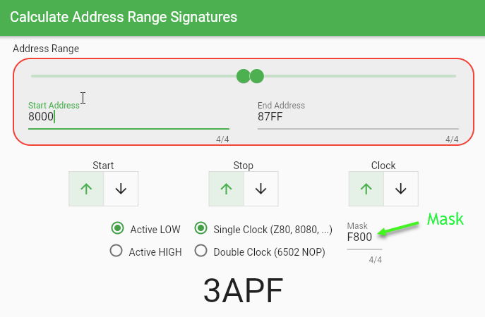
Given this decoding only uses A15..A11 we need to apply a mask of F800 when using the signature calculator...

CaptureRAMSig.png


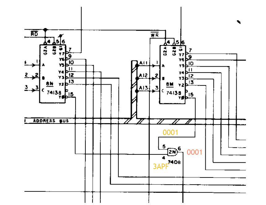
So the 3APF chip select signature is spot on but it isn't appearing at the 2114s... Tracing to back across the board to the AND gate at 2N... we expect pin 6 to also show 3APF... however it shows 0001 (i.e. stuck high)... the AND gate has gone to heaven... time to warm up the soldering iron again.

CarptureROMDecode.png
 

NivagSwerdna

Active member
Feedback
1 (100%)
Credits
840CR
So replaced 2x 2114 at 7N and 7P but reads and writes are not working correctly... they sort of work but not quite... it's like there is data bus connection which is odd since I can read the ROMs OK... must be a problem on Writes...

I tried by swapping with the 2114s at 3F and 3H but that is worse. Put all 2114s in my rather rudimentary chip tester and the originals (3F/3H) test bad so they go in the bin; the two I found lying around test good so will continue with those at 7N and 7P.

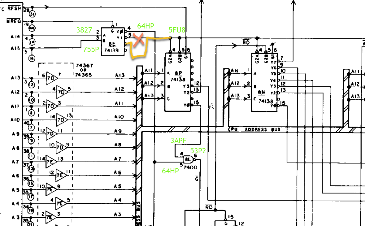
Took a few signatures for the logic that controls the buffers at 8F/8H... maybe they are firing at the wrong time?

CaptureRAMConflicts.png


I might have to ponder on this for a while. Note that 8E pin 5 is cut and its previously routed output feed from pin 6.... this is a moon cresta hack.
 

NivagSwerdna

Active member
Feedback
1 (100%)
Credits
840CR
Macro said:
moon cresta normally has ram and object ram at different addresses to galaxian, but I am sure you know that already.

8000-83FF, 9000-93FF and 9800-98FF
Yeap. Just working through this board...

ROM 0000-3FFF has active low... Sig 64HP

7P/7N RAM 8000-87FF (mirrored) active low......... Sig 3APF

ROM OR 7P/7N RAM i.e. 0000-3FFF OR 8000-87FF has Sig 5P32...

Therefore the enable signal for the 8F/8H is "Not either ROM nor 7P/7N RAM" which makes sense.

So measured signals match the theoretical ones.
smiley1.gif


Will remove the buffers at 8F and 8H and see if that makes a difference.

NivagSwerdna2022-07-24 19:03:45
 

NivagSwerdna

Active member
Feedback
1 (100%)
Credits
840CR
Got slightly side tracked as I could not realiably read and write to system memory (8000-83FF), it appeared that I could write sometimes but a good deal of my writes were going missing and hence implying bad memory... tried many things with my in-circuit tester including changing timings and banging my head on the wall and eventually decided to hook up the oscilloscope...

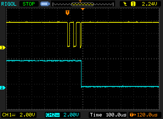
CaptureWREN.png


I set the tester to write 4 bytes and then pause briefly on a loop, the scope trace shows the RAM enable and the WEN (Write Enable line). If I got lucky then the four writes would occur during WEN but if I was unlucky then the WEN would clobber my writes; in the image above I get about two and half writes done before I get told to get lost. When WEN goes low the decoder at 8M is disabled and accessing the system RAM is not possible.

Now with my tester installed I am only accessing system RAM so WEN should never come into the equation; indeed if you look at the schematic...

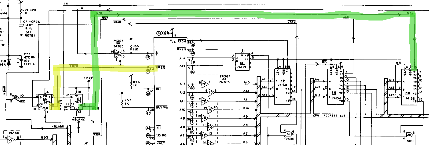
CaptureWENCircuit.png


Although not completely obvious the WEN line relates to VRAM. Specifically the intention is that if an attempt is made to write to VRAM during a period where the screen is being rendered i.e. HBLANK=0 then the CPU will be presented with a LOW on pin 24 (nWREQ aka nWAIT) and will defer memory operations until that condition is cleared, the 2nd gate in 6S disables the write address decoding during this period.

Now for my four writes I am never going near VRAM address ranges so this circuit should not be firing but a close inspection...

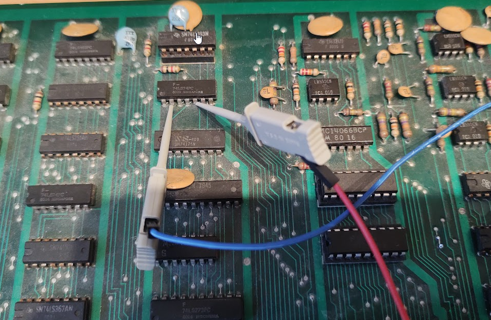
CaptureWRENFlip.png


The 3R NOR Gate is good but the dual D Flip Flop at 6S is showing pulses on pin 5 even though it's input is always LOW. So the first gate of the 7474 is knackered... time to warm up the soldering iron again!

This is a very interesting fault which I haven't seen before... the over excited nWREQ/WEN logic was running over my memory access. In real life this would cause massive delays by the introduction of long periods of wait for the CPU... glad I caught it now.

NivagSwerdna2022-08-01 20:21:50
 

NivagSwerdna

Active member
Feedback
1 (100%)
Credits
840CR
Socketed and replaced 74LS74 at 6S

... and as if by magic...

!m8000*0400

m: 8000=OK


i.e. Memory Short test of 8000 to 83FF... tests Good


smiley1.gif


NivagSwerdna2022-08-01 19:56:38
 

NivagSwerdna

Active member
Feedback
1 (100%)
Credits
840CR
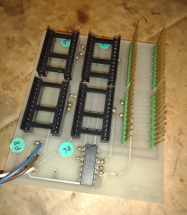
I am starting to think about graphics... the PCB came with a small daughterboard which plugs into sockets 1KL and 1JH...

CaptureROMBoard.png


The board is connected via three wires for some kind of bank switching.

I wasn't supplied with any ROMs but I would speculate that the intention is for 4x 2716 in these sockets?

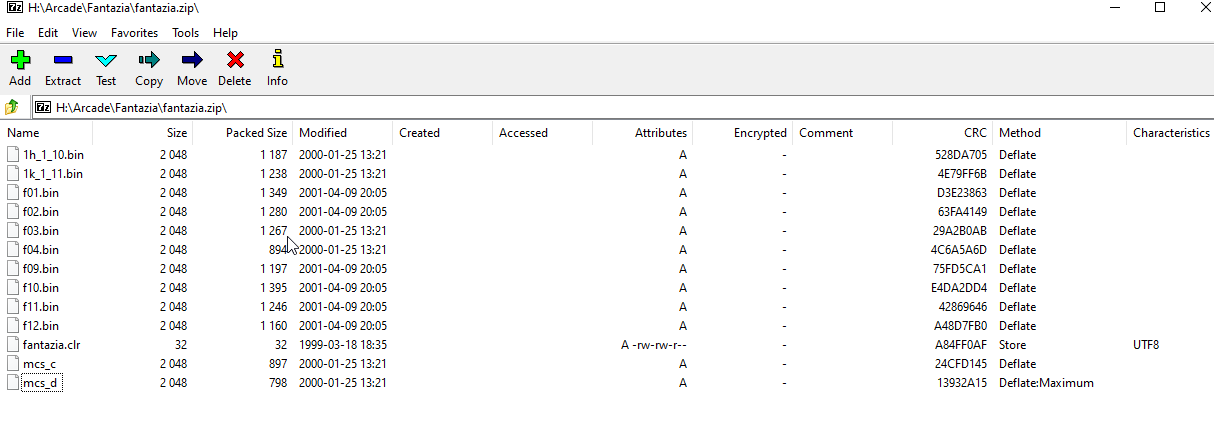
I assumed this was a Fantazia but looking at the fantazia.zip I see two images 1k_1_11.bin and 1k_1_10.bin both with 2048K bytes.

CaptureFantazia.png


Something fishy here...
 

NivagSwerdna

Active member
Feedback
1 (100%)
Credits
840CR
Did more googling....

CaptureFantazia2.png


Another ROM set with the same name but includes two more files! I notice that the colour PROM checksums are different too... hopefully this one is more trust worthy! The main code looks identical to the other one.

CRCs seem to match MAME too..

ROM_START( fantazia )

ROM_REGION( 0x8000, "maincpu", 0 )

ROM_LOAD( "f01.bin", 0x0000, 0x0800, CRC(d3e23863) SHA1(f0a6f7491fdf8aae214f40078b29b7aecdcf2f1e) )

ROM_LOAD( "f02.bin", 0x0800, 0x0800, CRC(63fa4149) SHA1(603ee6d4d2952cc08b3f6e98b1a2053671875e44) )

ROM_LOAD( "f03.bin", 0x1000, 0x0800, CRC(29a2b0ab) SHA1(e9fc7161d0566e36307c45b7132e2262c0af4845) )

ROM_LOAD( "f04.bin", 0x1800, 0x0800, CRC(4c6a5a6d) SHA1(366516f63c9b5239e703e4dfb672659049ddbf44) )

ROM_LOAD( "f09.bin", 0x2000, 0x0800, CRC(75fd5ca1) SHA1(45f2dd33f0e437cb95d9373f86490e5432338737) )

ROM_LOAD( "f10.bin", 0x2800, 0x0800, CRC(e4da2dd4) SHA1(7a53efd5b583f656c87b7d7a5ba7c239ced7d87b) )

ROM_LOAD( "f11.bin", 0x3000, 0x0800, CRC(42869646) SHA1(a3640b2ace31ce99c056bc14d1d96f3404698d6a) )

ROM_LOAD( "f12.bin", 0x3800, 0x0800, CRC(a48d7fb0) SHA1(6206036a9d85e87fb7f8a88c17bfe090fc70caf4) )

ROM_REGION( 0x2000, "gfx1", 0 )

ROM_LOAD( "1h_1_10.bin", 0x0000, 0x0800, CRC(528da705) SHA1(d726ee18b79774c982f88afb2a508eb5d5783193) )

ROM_LOAD( "mcs_d", 0x0800, 0x0800, CRC(13932a15) SHA1(b8885c555c6ad7021be55c6925a0a0872c1b6abd) )

ROM_LOAD( "1k_1_11.bin", 0x1000, 0x0800, CRC(4e79ff6b) SHA1(f72386a3766a7fcc7b4b8cedfa58b8d57f911f6f) )

ROM_LOAD( "mcs_c", 0x1800, 0x0800, CRC(24cfd145) SHA1(08c6599db170dd6ee364c44f70a0f5c0f881b6ef) )

ROM_REGION( 0x0020, "proms", 0 )

ROM_LOAD( "fantazia.clr", 0x0000, 0x0020, CRC(a84ff0af) SHA1(c300dc937c608d2d1c113ca7a53c649472c72379) )

ROM_END

NivagSwerdna2022-08-03 21:20:54
 

cliff_poole

Active member
vacBacker
Feedback
6 (100%)
Credits
1,069CR
Does the colour PROM checksum match Moon Cresta ?. It was suggested by Macro earlier. That ROM board with the three wires looks just like Moon Cresta.
 

NivagSwerdna

Active member
Feedback
1 (100%)
Credits
840CR
cliff_poole said:
Does the colour PROM checksum match Moon Cresta ?. It was suggested by Macro earlier. That ROM board with the three wires looks just like Moon Cresta.
I'll have to dump it and see what I have got. According to MAME the mooncrst colour PROM has CRC 6a0c7d87 but the one I just downloaded has a84ff0af... I'll get on that.
 

NivagSwerdna

Active member
Feedback
1 (100%)
Credits
840CR
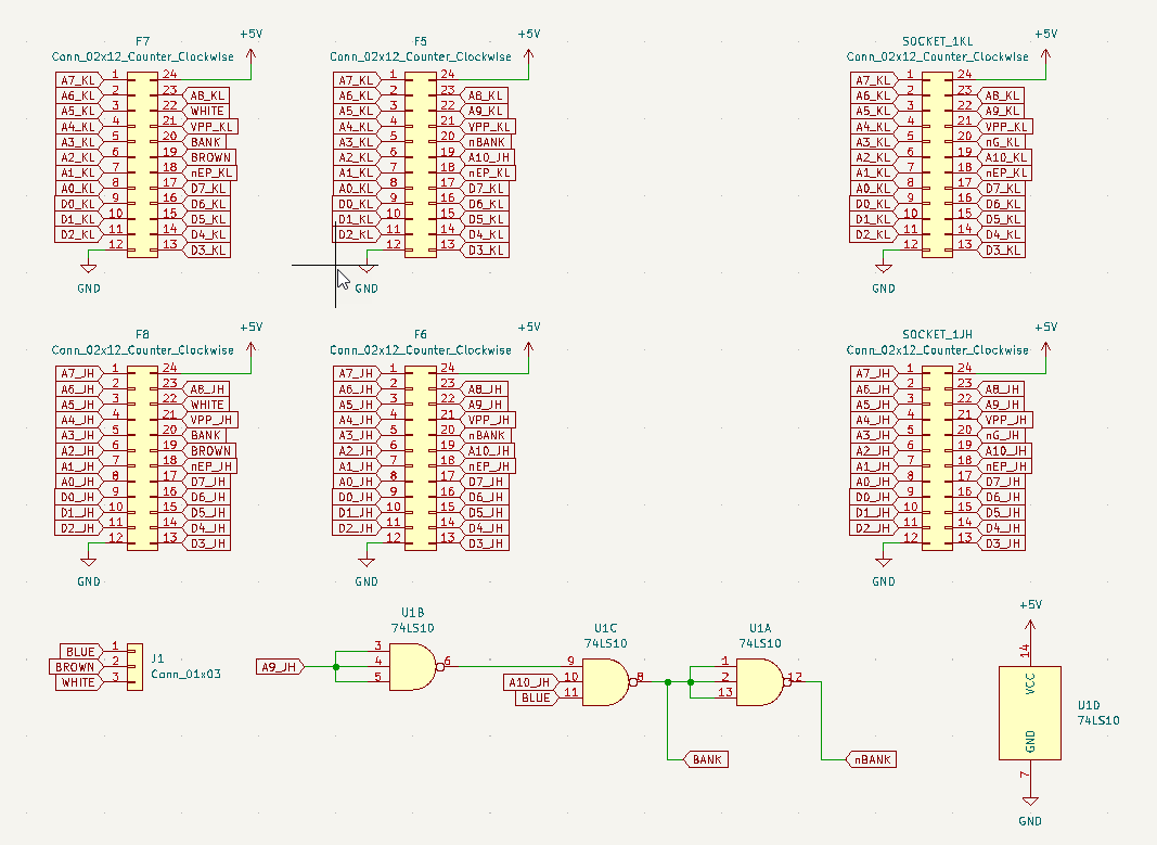
I drew a quick schematic of the ROM daughter board...

CaptureROMBoardSchematic.png


I'm tempted to make a neater replacement but it's probably not worth the effort. Looking at the logic it seems about right... Brown, White and Blue go to the 74LS259 at 9M to pins 4, 5 and 6. i.e. these map to 1-bit registers at A000, A001 and A002 respectively. (Would be 500x in Galaxian but switched in the memory map for mooncrst).

The intention here is that if Blue=0 (i.e. A002=00) then the ROM sockets work as per Galaxian.

If Blue=1 AND A9=0 and A10=1 addressed then swap in a new ROM pair where A9=White and A10=Brown.

This matches the MAME source...

/*** Moon Cresta ***/

void galaxian_state::mooncrst_extend_tile_info(uint16_t *code, uint8_t *color, uint8_t attrib, uint8_t x, uint8_t y)

{

if (m_gfxbank[2] && (*code & 0xc0) == 0x80)

*code = (*code & 0x3f) | (m_gfxbank[0] << 6) | (m_gfxbank[1] << 7) | 0x0100;

}

So in the interim I can ignore banking completely and put 2x 2716s in the Galaxian Sockets... should work for the early testing at least.
 

Macro

Active member
vacBacker
Feedback
4 (100%)
Credits
2,009CR
For the multigame I just dumped out the 5 different options with the relevant graphics and then paged those in as needed. simplifies the logic and wiring (and I had tons of eprom space anyway - it uses 27256s)
 

NivagSwerdna

Active member
Feedback
1 (100%)
Credits
840CR
Macro said:
For the multigame I just dumped out the 5 different options with the relevant graphics and then paged those in as needed. simplifies the logic and wiring (and I had tons of eprom space anyway - it uses 27256s)
Which multigame?
The banking logic is required in game here to swap out the enemy sprites as the game progresses; it only affects the higher ranges so the earlier sprites are unaffected hence the check on A9 and A10.
 

NivagSwerdna

Active member
Feedback
1 (100%)
Credits
840CR
Macro said:
I simplified the banking logic by making 5 complete graphic pages, each with the relevant higher range sprites. it's more compatible with other banked games that way.
ah. I see! That's very clever!
smiley1.gif
NivagSwerdna2022-08-06 11:55:47
 

NivagSwerdna

Active member
Feedback
1 (100%)
Credits
840CR
OK so you piqued my interest...

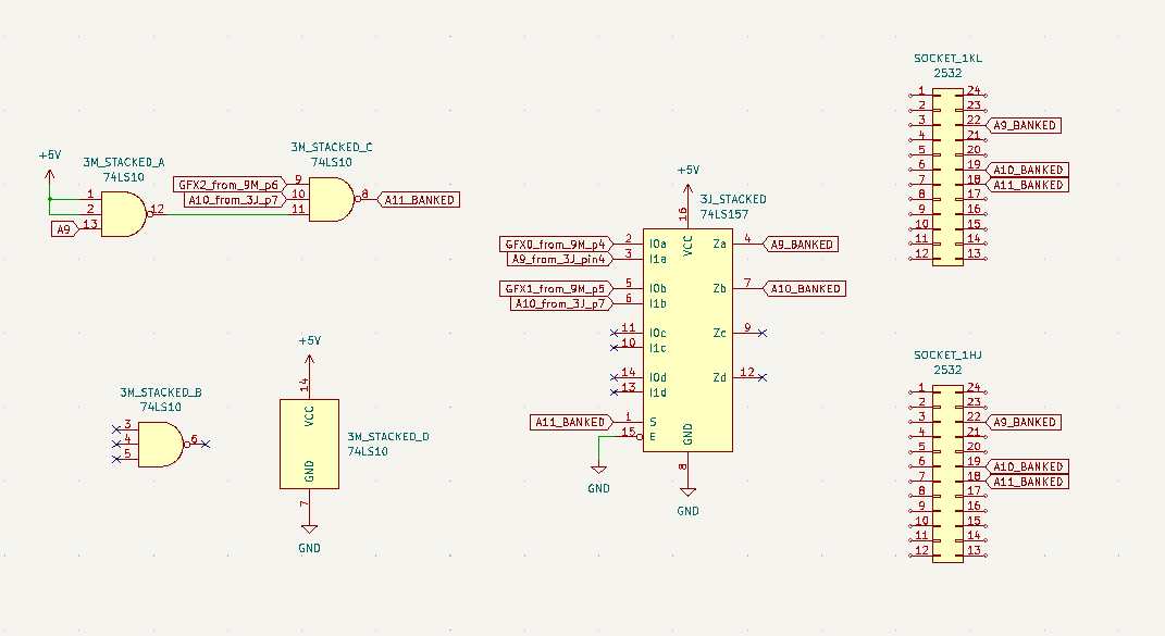
My other Moon Cresta (described in another fix log) uses a pair of 2532s with the extra address logic provided by stacking a 74LS10 on top of 3M and a 74LS157 stacked on top of 3J and then various bodge wires etc...

CaptureMCGFXSchematic.png


So the scheme is slightly different but almost the same. The nice thing about this approach is it uses only 2 ROMs (2532s) whereas the existing scheme uses 4 ROMs (2716s)... Although I have a ready supply of 2716s it's tempting to rework this as I think the daughter board is a bit crusty.
 
Top